


- ホーム
- インダストリー
- 検査 & 計測
- Technical Papers
- Design of a Testing Apparatus for AIR Navigation Vor Signals
日本語
Wu Guangbo, Liu Liansheng
Fundamental Experiment Center,
Civil Aviation University of China
Application
Testing of air navigation equipment, signal generation, and signal collection.
Challenge
In the testing of avionic equipment, it is required that multifunctional automatic testing systems be constructed with limited resources. As is well known, airborne electronic equipment uses numerous complex signals, including low-frequency and high-frequency signals, continuous and discrete signals, and even non-electric signals. Conventional testing systems, typically composed of separate instruments, are costly but have a low degree of test automation and low expandability. With the development of the civil air transportation industry, most airborne electronic equipment has been highly digitized and integrated, making it impossible to test or check the equipment manually. Hence conventional testing instruments have failed to meet practical needs. By contrast, signal processing mechanisms based on software-defined radio are advantageously flexible and open and therefore meet said needs. Such advantageous features also facilitate teaching, learning, and research.
Solution
This study is directed to air navigation VOR signals by way of example. Research was made on the principle of VOR navigation, followed by analyses and modeling of VOR composite signals. The time-domain data of waveforms can be conveniently expressed and calculated with equations. In this study, the time-domain data obtained were input into a DAC to generate simulated waveforms, which were then up-converted to the desired frequency. Existing analog signals were collected with a PCI-9846 high-speed digitizer, and the data collected was displayed in real time or stored as files for subsequent use and analysis. It has been verified that the application of software-defined radio to an automatic testing system can save costs significantly, simplify the system, and increase efficiency. In addition, the performance indices of the digitizer satisfy practical needs.
Air navigation VOR (Very High Frequency Omnidirectional Range) signals are collected with the PCI-9846 high-speed digitizer from ADLINK Technology, subjected to time-domain and frequency-domain analyses, and then demodulated to restore directional information. Thus, accuracy of the signals can be rapidly checked. It has been verified that the application of software-defined radio to an automatic testing system can save costs significantly, simplify the system, and increase efficiency. Moreover, the performance indices of the digitizer satisfy practical needs.
In the testing of avionic equipment, it is required that multifunctional automatic testing systems be constructed with limited resources. As is well known, airborne electronic equipment uses numerous complex signals, including low-frequency and high-frequency signals, continuous and discrete signals, and even non-electric signals. Conventional testing systems, typically composed of separate instruments, are costly but have a low degree of test automation and low expandability. With the development of the civil air transportation industry, most airborne electronic equipment has been highly digitized and integrated, making it impossible to test or check the equipment manually. Therefore, developed countries are now using automatic testing equipment to perform related tasks. [1][2]
The fundamentals of software-defined radio consist of a general-purpose, standard, modular hardware platform which carries out the various functions of a radio station by means of software programming, as opposed to conventional hardware-based, application-oriented radio station design methods [3]. An automatic testing system has higher requirements for the flexibility and comprehensiveness of the signal source, so the traditional signal generators no longer meet these needs [4]. By contrast, signal generators based on software-defined radio are advantageously flexible and open and are therefore suitable for use. These advantageous features also facilitate teaching, learning, and research.
In this study, the PCI-9846H of ADLINK is applied to the testing and calibration of the signal source of an automatic testing system, and air navigation VOR signals are collected and processed to restore basic information. It has been proved that the performance indices of the digitizer satisfy practical needs.
1.VOR Signal
Basically, a very high frequency omnidirectional range signal provides a complex radio signal to an airborne VOR signal receiver, which demodulates the signal to determine the magnetic bearing, i.e., VOR bearing, of the VOR signal station on land in relation to the aircraft [5]. The spatial VOR composite signal received by the airborne receiver includes a reference-phase signal and a variable-phase signal. Orientation can be accomplished by comparing the phases of these two signals. The operating frequency of a VOR signal ranges from 108MHz to 117.95MHz, with a channel spacing of 0.05MHz.
1.1 VOR Reference-Phase Signal
A VOR reference-phase signal includes a radio-frequency (RF) carrier and a 9960Hz subcarrier. The frequency of the RF carrier ranges from 108MHz to 117.95MHz. The 9960Hz subcarrier is frequency-modulated by a 30Hz reference signal, with a modulation index of 16, as expressed by the following equation:

where  is the modulation index of the subcarrier on the RF carrier,
  is the frequency of the subcarrier, is
  the modulation index on the subcarrier,
  is the frequency of the baseband signal, and
  is the RF frequency.
A reference-phase signal has a constant signal radiation intensity in every radial direction, i.e., from 0° to 360°, and the phase of the 30Hz signal is also radially constant from 0° through 360°. Therefore, in terms of radiation patterns, the horizontal directivity pattern is a circle.
1.2 VOR Variable-Phase Signal
A variable-phase signal only includes a simple RF carrier, whose frequency ranges from 108MHz to 117.95MHz. Two pairs of orthogonal sideband antennae radiate a sine modulated sideband wave and a cosine modulated sideband wave respectively, and the field intensities of these waves vary regularly at 30Hz. Thus, a 30Hz amplitude modulated wave featuring regular sinusoidal variation is generated in the space, as can be expressed by:

where  is the current VOR radial azimuth.
1.3 Composite Signal
A spatial composite signal is a superposition of a reference-phase signal and a variable-phase signal, as shown in Figure 1 and expressed by the following equation:

A receiver demodulates the composite signal and calculates the phase difference of the two component signals to obtain directional information.[5,6]
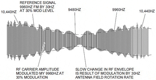 Figure 1. Spatial Composite Signal.
2. System Implementation
A GPP (General-Purpose Processor)-based system structure is used, and digital signals are directly processed by an industrial personal computer (PC). A radio system of this kind does not have the physical look of a radio station and provides radio communication solutions entirely from the perspective of software. A GPP is not a real-time synchronization system and therefore is not suitable for real-time processing of signals obtained by strictly timed sampling. A GPP can achieve synchronization to a certain degree only via interruption. Nevertheless, due to its openness, flexibility, programmability and advantages in human-machine interface, a GPP-based system approximates the ideal software-defined radio system and is perfect for testing, teaching, learning, and research purposes.
The aforesaid system uses pipeline-like connections, wherein the directions of the pipelines are consistent with signal flows. The pipeline-like connections, featuring high efficiency, a short time delay and a high processing rate, can compensate, to some extent, for the low signal processing speed of the GPP. However, with the modules in the system being physically connected and closely coupled together by circuits and having a low degree of independence from one another, a change in system functions will require the addition of a new module or removal of an existing module, and the corresponding modules, if not the entire structure, must also be changed. In this study, the pipeline-like structure as shown in Figure 2 is chosen because the design objective is to test and calibrate the signal source of a testing system in which signals are relatively stable and need not be changed frequently [7]. Signal generation and processing are performed by the aforementioned industrial PC. An arbitrary waveform generator (AWG) realizes waveform output (a digital up-converter card is required in case of high frequencies). For radio transmission and receiving, an additional antenna and RF amplifier will be needed. Signal collection and A/D conversion are accomplished by ADLINK's PCI-9846 high-speed digitizer. The conversion results can be displayed in real time or saved as waveform files for subsequent processing.
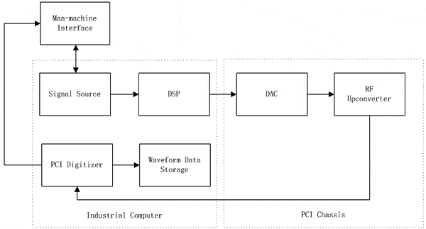 Figure 2. System Block Diagram.
2.1 Signal Source
Medium-frequency signals are generated by the arbitrary waveform generator. The arbitrary waveform generator used is one capable of onboard signal processing (OSP), with 16-bit resolution and -91 dBc close-in spurious-free dynamic range (SFDR), and can provide an instrument quality standard for the required digital up-conversion and baseband interpolation applications. Having all the desired functions, the AWG can also generate general-purpose electronic testing signals, with a maximum output range of 12Vpp, a resistive load of 50Ω, and a highest frequency of 43MHz. The up-converter card is built-in with a 2.7 GHz up-converter, featuring high real-time bandwidth, a stable time base, and a precision as high as ±50ppb. In RF generation applications, the up-converter card is tightly integrated with a modular function generator to generate a signal whose frequency ranges from 50kHz to 2.7GHz, with an adjustable gain range of 130dB. The arbitrary waveform generator generates high-frequency VOR signals, which are sent to the up-converter for up-conversion to the desired very high frequency band.
A PXI card is installed in the PXI chassis. With a PXI-PCI extension kit, PXI modules can be controlled via a computer using a fully transparent MXI-4 link connected by a copper cable. Through a bridge built on a PCI-PCI high-bandwidth connection, the MXI-4 enables remote control over the PXI system through the PCI interface of the computer.
2.2 Data Acquisition
Data acquisition is carried out by the ADLINK PCI-9846 high-speed digitizer. The ADLINK PCI-9846 is a 16-bit 4-channel digitizer with a sampling frequency of 40MHz, designed specifically for high-frequency, large dynamic range signals, and allowing a maximum input frequency of 20MHz. The analog input measuring span can be set at ±1V or ±0.2V via software, and a 50 ohm input impedance can be used in order to deal with high-speed high-frequency signals. A highly linear 4-channel 16-bit A/D converter is provided for ideal adaptation to large dynamic range signals such as radar, ultrasonic waves, and software-defined radio.
Equipped with onboard memory as large as 512MB, the PCI-9846 can record waveforms for a long period of time without being limited by the transfer rate of the PCI bus. Digitized signal data are stored in the onboard memory before transmission to the main memory. Data transmission is carried out through SG-DMA (Scatter-Gather Direct Memory Access) so that not only can a higher data transfer rate be provided, but also the system memory can be used more effectively. If the data transfer rate of the digitizer is lower than the available PCI bus bandwidth, the onboard sampling point first-in first-out memory of the PCI-9846 allows data to bypass the onboard memory and be directly transferred to the host memory in real time.
The PCI-9846 can be triggered in a flexible manner, such as by software triggering, external digital triggering, analog triggering through an arbitrary analog channel, and PXI bus triggering. The various triggering options make the PCI-9846 highly adaptive to practical needs. In the post-triggering, delayed triggering, pre-triggering and middle-triggering modes, data around the triggering event are collected. PCI-9846 also allows repeated triggering so that data sections with very short time intervals can be collected. Thanks to the multiple triggering options provided by the PXI backplane, PCI-9846 can readily implement synchronization between a plurality of modules. And thanks to the PXI trigger bus, PCI-9846 can output triggering or time-base signals to the PXI trigger bus when set as "master" and receive triggering or time-base signals from the PXI trigger bus when set as "slave". The PXI backplane also provides a precise 10 MHz signal which can serve as a time-base signal source.
PCI-9846 includes a precise low-temperature drift onboard reference, which not only can function as a stable calibration source but also ensures the stability of data acquisition over a relatively large temperature range. The automatic calibration process is executed by means of software, without need for any manual adjustment. Once the calibration process is completed, the calibration information is stored in an onboard EEPROM (Electrically Erasable Programmable Read-Only Memory). The calibration values can be loaded from the board when needed. [10]
2.3 Software
LabVIEW is a testing system software development platform based on G language (Graphics Language) [11]. The generation of signals, the invocation of the digitizer and the processing of digital signals are all performed in the LabVIEW2010 environment.
Due to limited machine functions, the program is divided into three parts: generation, collection and processing. Waveform data are calculated according to the results of signal modeling (see "1.3 Composite Signal") and are saved to a file. The waveform generation program begins by reading the waveform data and writing the waveform data into the arbitrary waveform generator. Then, the arbitrary waveform generator is called to generate the desired signals. Under the control of the DAQPilot-related modules, the digitizer begins signal collection. The collected data are stored into a file for subsequent use. The demodulation program calls the above-mentioned waveform file and performs demodulation and operations on the file, thereby completing signal analysis. Figure 3 shows a block diagram of the signal generation and collection program, and Figure 4 shows a block diagram of the demodulation and operation program.
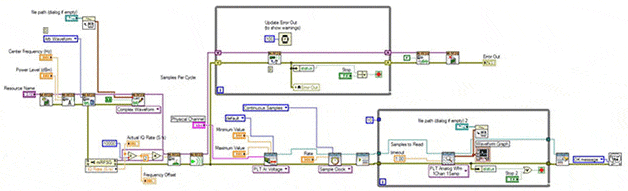 Figure 3. Signal Generation and Collection Program.
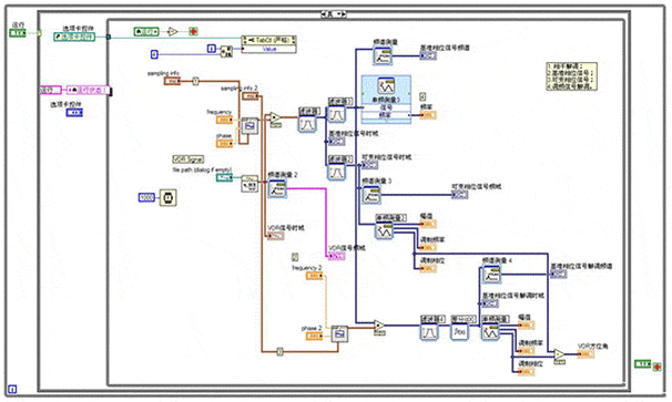 Figure 4. Signal Demodulation Program.
3. Operating Results
Hardware components are connected according to the designed hardware structure, and waveform information is set. The baseband signal is a 30Hz sine wave. The frequency modulated (FM) subcarrier is at 9960Hz, with a frequency deviation of 480Hz and a modulation index of 0.3. Considering machine performance and the operating time, the VOR signals are at 1MHz by way of example. The waveform obtained from calculation is saved into a file so as to be called by the waveform generation program. The waveform generation program begins with equipment initialization and parameter adjustment. Then, the card address is set. The power is -10dBm, the center frequency is 1MHz, and the mode is "Arb Waveform". Once the waveform file is called, IQ modulation is applied, wherein I is the modulation signal and Q is 0. When writing data, the same sampling rate as that used in the generation process is selected to ensure that the signals generated have the correct frequency spectrum. [12]
While the signal generation module continues operating, the digitizer is called to perform signal collection. Similarly, a virtual channel must be set. The measuring span is set at ±1V, and the signal type is "AI Voltage". The sampling frequency must satisfy Nyquist's theorem and is set at 8MHz in this study. The sampling clock is set at "Continuous Samples", with the continuation time being 1 second. The sampled data can be displayed in the waveform diagram in real time and, by means of "Write waveform data into file.vi", saved into a file for subsequent use.
In order to realize signal measurement and verification, the collected waveform must be demodulated to restore the corresponding information. The collected spatial VOR composite signal is subjected to interference demodulation to obtain the outside envelope of the spatial composite signal, which includes a 30Hz variable-phase signal and a 9960Hz FM subcarrier. The 30Hz variable-phase signal can be directly obtained with a 30 Hz filter. The time-domain and frequency-domain waveforms, as well as the frequency, phase, amplitude, and similar information, of the 30Hz variable-phase signal can be seen on the front panel. The 9960Hz subcarrier is filtered and frequency discriminated to obtain the 30Hz reference-phase signal, whose corresponding parameters can also be seen on the front panel. The phase difference between the reference-phase signal and the variable-phase signal provides information of the current direction, which information is read as the VOR azimuth. Figure 5 shows the front panel after the aforesaid operation. During program operation, all the tab pages can be displayed in turn. By pressing the "Pause" button on the lower right corner, the current tab page can be locked.
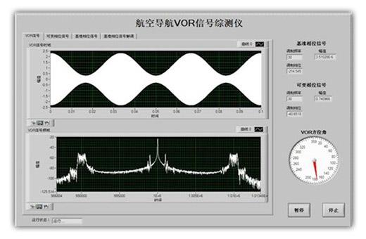 Figure 5. Front Panel of the Testing Apparatus.
Conclusions
Nowadays software-defined radio technology has found extensive application in military and civil communications. Testing equipment based on this technology is open and flexible and is therefore more promising than conventional equipment. On the other hand, digitizers are the key to transition from analog signals to digital signals. It has been verified that the PCI-9846 high-speed digitizer of ADLINK is easy to install, has a user-friendly interface, can be conveniently used in the LabVIEW environment, is well capable of accurate collection of complex analog signals and analog-to-digital conversion, and can store the collected signals into waveform files for later use. Due to technical limitations and the performance of the computers used, this study was unable to sample at higher frequencies and conduct more signal processing experiments. Hence, further research and improvement efforts are called for.
References:
[1] Dong Qinpeng, Xiong Huagang. Design and Realization of Automatic Test System Based on Aircraft Electronic Equipment. Modern Electronics Technique [J], 2008, 21, 146-149.
[2] Lu Yiqing. New generation Avionics Testing Equipment. Foreign Electronic Measurement Technology [J], 2000, 1, 8-11.
[3] Baidu Encyclopedia. Software-Defined Radio [OL]. [2010.11.27]. http://goo.gl/lKi0D.
[4] Dong Qinpeng, Xiong Huagang. Design and Realization of Automatic Test System Based on Aircraft Electronic Equipment. Modern Electronics Technique [J], 2008, 21: 146-149.
[5] Zheng Lianxing, Ni Yude. DVOR VRB-51D Doppler Omnidirectional Signal [M]. Beijing: China Civil Aviation Publishing House, 1997: 8-15.
[6] Rockwell Collins Company. VOR-700 Receiver Component Maintenance Manual. 17th Revision. Printed in the United States of America, 2006: 71-76.
[7] Xiang Xin. Theory and Technology of Software-Defined Radio [M]. Xi'an: Xi'an University Press, 2008:14-19.
[8] ADLINK Technology Inc. PCI/PXI-9816/26/46 4-CH 16-Bit 10/20/40 MS/s Digitizer with 512 MB SDRAM User's Manual. ADLINK Technology Inc, 2009: 11-12.
[9] Dai Pengfei, Wang Shengkai, Wang Gefang. Testing Engineering and LabVIEW Applications [M]. Beijing: Publishing House of Electronics Industry, 2006: 13-15.
[10] Song Guan, Guangbo Wu. Study on a VOR Signal Generator Based on Software-Defined Radio [C]. ICTIS2011, Wuhan.