

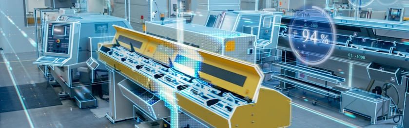


Shaping the Future of Semiconductor Packaging and Testing
PC-based Motion Control that Enables High-Precision, High-Efficient Performance
The semiconductor industry has been booming in recent years which is expected to reach a healthy CAGR of over 6% by 2026, primarily due to the wide extent of applications in trending fields such as IoT, 5G, AI and consumers electronics that is creating sustained demand for semiconductors.
However, with the continuous miniaturization of the semiconductor manufacturing process, chip designs are becoming lighter, thinner, and have three-dimensional heterogeneous integration, with the process inevitably moving toward having higher precision and high speed to further enhance manufacturing productivity. ADLINK’s integrated machine vision and motion control system overcomes these challenges encountered by the semiconductor industry. This solution maintains quality and accuracy with overall performance optimized up to 20% with a simpler operating interface while saving up to 25-50% of the cost.
Why ADLINK?

ADLINK offers advanced image capturing, motion compensation, and rich I/O solutions to deliver accurate positioning for precision analysis.

ADLINK’s motion control supports motion path optimization with rapid response time to reduce overall operating time.

A PC-based system ensures exceptional compatibility between motion control and visual capture to achieve multiple workspace/axis synchronization.

ADLINK’s motion control solution features the APS SDK, an intuitive platform that simplifies secondary development for users. It offers at least 15 motion control functions, especially for applications such as laser dicing and die bonding.
Proven Success Cases
-
Laser Dicing
ADLINK’s laser dicing solution overcomes the complex dicing process to meet modern chip requirements with quick positioning, sensor matching and laser power intensity control.
Learn more
-
Probe Testing
ADLINK’s probe testing solution integrates simulation into a motion control card to achieve the most precise command control up to 0.1 μm that will not damage wafers.
Learn more
-
Die Sorting
ADLINK’s die sorting solution demonstrates perfect multi-axis integration, enabling simultaneous all axis control and quick picking of qualified or defective wafers.
Learn more
-
Die Bonding
ADLINK’s die bond solution achieves more accurate positioning and dispensing of the precise amount of adhesive. This solution ensures chip quality and improves productivity by up to 20%.
Learn more
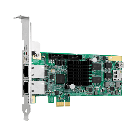
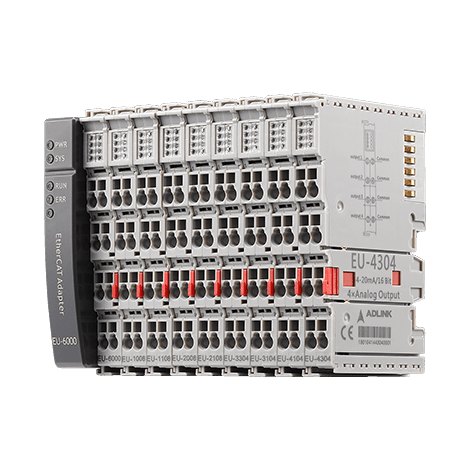
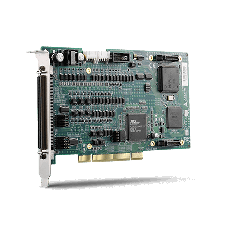
Offerings
-

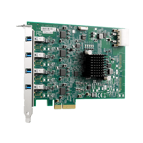
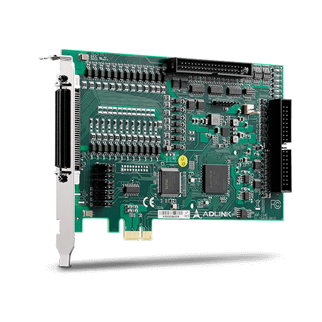
Motion Controller Card
-

-

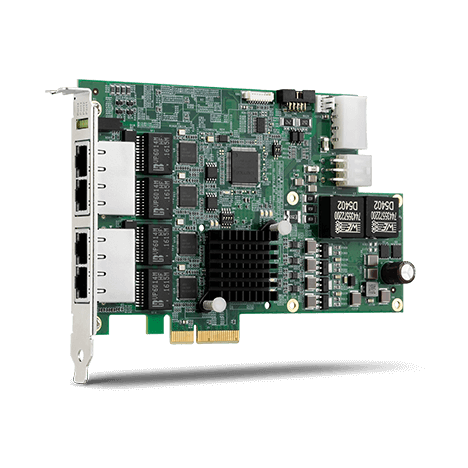
Vision Frame Grabbers Card
-