|
Increasing Image Acquisition Rates for Bandwidth Hungry Applications Neil Chen, Product Manager, ADLINK Technology |
|
| Bandwidth Hunger: | |
|
Electronics component manufacturers must continually improve productivity and quality to remain competitive. Motion control and machine vision play an important role in this effort by providing automated inspection capabilities that are more reliable and scalable than legacy methods. As manufacturers require increased image throughput and more sophisticated image processing, transferring the data from the camera to the PC, or bandwidth, often becomes a limiting factor that must be addressed. Standard VGA resolutions and a 30 frame/second capture rates were sufficient for most production lines in the past. Industry requirements are now demanding an increase in the dimensions scanned (e.g. line scan (is line scan an increase or decrease in "dimension"), and 3D inspection, (should we also mention OCR, barcode, 3D barcode, etc.?)), and increase in the production line conveyer speed, and more complex image processing.. Meanwhile, bandwidth has remained the main bottleneck for PC-base machine vision systems. Camera Link, a new camera standard, was introduced to address the bandwidth issue. Combined with PCI Express bus, Camera link image solutions provide unprecedented data transmission for machine vision applications. This article will examine "bandwidth hungry" vision applications and how PCI Express, Camera Link and FPGA technologies have been implemented to increase image acquisition and processing rates. Feeding the Demand |
|
| Figure 1: Computer-based Machine Vision System | |
|
Figure 1 shows the primary components of a typical computer-based machine vision system. These components include a camera with lighting, cabling, plug-in frame grabber card, and computer. Camera Link was developed as an open specification for cameras and frame grabber cards to be used in such machine vision systems. The Camera Link interface specification was defined by the Automate Imaging Association (reference), an industry group consisting of industrial camera, cable, and frame grabber card manufacturers. Camera Link utilizes LVDS (Low Voltage Differential Signaling) technology to transmit digital data. Both a parallel-to-serial transmitter and a serial-to-parallel receiver are used to transmit image data.
|
|
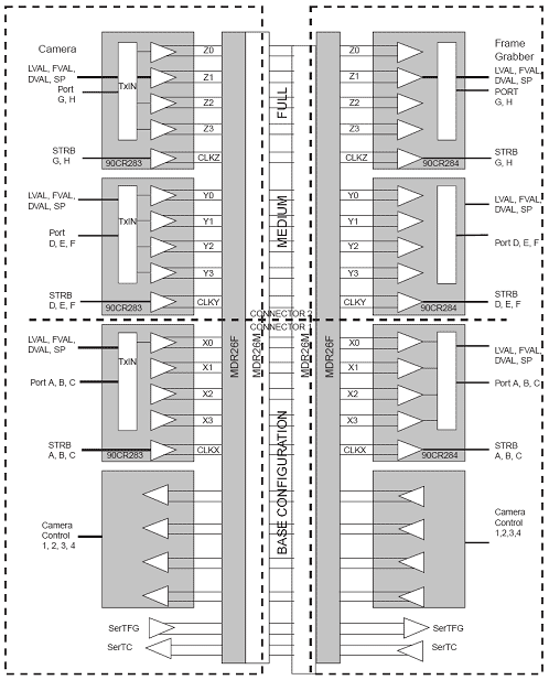
| Figure 2: Camera Link Hardware Structure (do we have a more "friendly" or "dumbed" down version of this graphic? This seems to be too much detail?) | |
|
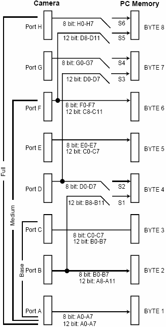
Camera Link As shown in Figure 2, the Camera Link standard provides for three configurations: base, medium, and full signaling modes. Image data from the camera is transmitted through a designated port to the corresponding port connected to the frame grabber. The base configuration consists of a set of transmitter/receiver pairs (24 bits of video data organized into three 8-bit ports: A, B, and C plus FVAL (frame valid), LVAL (line valid), DVAL (data valid), and spare signals), one clock signal, one serial communication channel, and four LVDS general-purpose camera control signals. The camera control signals are typically used with external triggering to capture images in real-time. The clock runs at rates between 20 to 85 MHz for an image data transmission rate of up to 2.04 Gbps. The medium configuration adds a second set of transmitter/receiver pairs to double the number of image data bits to 48 bits, which also doubles the number of 8-bit ports to six: A, B, C, D, E, and F). The image data transmission rate is also doubled to 4.08 Gbps. The full configuration further increases the number of image data bits to 64 bits for eight 8-bit ports: A, B, C, D, E, F, G, and H, and improves image data transmission rates to 5.44 Gbps. The Camera Link data routing is illustrated in Figure 3. (again, this seems like too much detail. Do Camera Link users really need to know this data? I thought it was more "plug and play") Of the currently available camera interfaces (such as analog connections, USB, FireWire, GigE), Camera Link provides the following advantages:
|
|
| Figure 3: Camera Link Data Routing | |
|
PCI Express Computer systems used in machine vision applications may now utilize the new PCI Express (PCIe) bus technology. The PCIe bus implements a serial packet-based protocol along with a switch-based topology to provide a high-bandwidth and robust point-to-point interconnects, which is a significant improvement over the predecessor PCI bus that offered bus-based connections where all the devices share the same 32- or 64-bit parallel bus. PCI Express bus maintains complete software compatibility with the existing base of operating systems, PCI drivers, and software, in addition to offering a scalable bus bandwidth. The physical layer of a PCIe link is a set as serial lanes in groups of 1, 2, 4, 8, 12, and 16. Each lane provides a 2 Gbps data transmission rate, which equates to a rate of 8 Gbps for a 4 lane link. The PCIe lanes also provide dedicated bus connections whereas bandwidth on the PCI bus is shared among all PCI devices and some system functions. In other words, the PCIe bus provides a dedicated link for image data transmission so that bandwidth is not shared during transmission. FPGA Based Image Processing As the amount of transferred image data increases, additional computing power is required in computer-based machine vision systems to maintain performance. As mentioned above, the majority of frame grabber cards support DMA to reduce CPU loading. Image processing on the host computer also loads the CPU. and can often lead to a system bottleneck. In the past, the only solution for image processing bandwidth was an perform on-camera or on-frame grabber image processing using an ASIC. However, ASIC solutions significantly increased development costs, delayed time-to-market, and limited processing flexibility. More recently, users have taken advantage of computer processor advances, such as multi-core, to increase image processing bandwidth However, processor solutions are limited in that they unable to integrate other hardware I/O signals, The use of a programmable component in the form of an FPGA (field programmable gate array) is able to address the limitations of both ASIC and processor based throughput solutions. An FPGA provides a set of logic elements whereby the pre-processing functions are executed on the frame grabber card, in parallel with the image acquisition and without causing any loading on the host CPU. The combination of the CPU and FPGA provides the proper balance between the performance and the cost of the machine vision system. Advantages of incorporating an FPGA include:
FPGAs are able to perform pre-processing functions such as shading correction, color space conversion, image rotation and look-up table operators. FPGAs can also provide enhanced images on-the-fly, ready for further processing on the host CPU, further supporting the concept of a proper balance between system performance and cost. |
|
| Combining It All: | |
|
The combination of Camera Link, FPGA, and PCIe technologies can provide the high bandwidth and high transfer speed required by advanced machine vision applications such as line scan and 3D inspection. For example, flat panel surface inspections typically require the simultaneous capture of multiple image channels. A PCI Express-based system supports multiple frame grabber boards and provides each board with a dedicated link to the host memory. Because the bandwidth of the PCI Express bus is guaranteed, each frame grabber can operate at full speed without sharing bandwidth. Thereby, the frame grabbers will not affect the performance of the other frame grabbers in the system, resulting in an inspection system with maximum throughput. Yet, as the image quality and image processing speed in machine vision applications increase, performance requirements may not be met solely through the host PC; the addition of an FPGA offers both increased performance and design flexibility. Camera Link offers the optimal solution for bandwidth, real-time signaling, and robust image transmission of the currently available machine vision solutions. Overall performance can be further improved when this technology is combined with other technologies, such as FPGA, to provide the system developers with the high-speed and high-resolution capabilities they need at a price they can afford. |
|
| more ADLINK Vision | |
 |
|